 This article is part of a larger project to build a multi-purpose board that can replace a Nokia 3310′s mainboard.
PGAs are quite common, but I don’t have one in my parts bin and I was curious about an idea I had for a while…
In the non-inverting configuration, the opamp gain is set by the two resistors ratio, and since one of them is grounded, I can add a resistor in parallel by connecting it to the MCU I/O and grounding the pin or setting it as an input to activate or deactivate it.
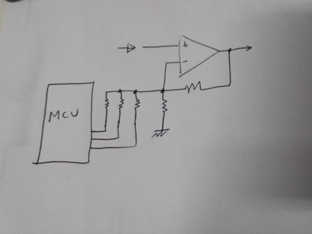
I looked around the web but couldn’t find anyone supporting/bashing my theory (if someone has links discussing this, please let me know), so I just tried it and it works! With the ATMEGA328P in the Trinket you must connect the resistors to analog pins, or else it will still load the amp too much when set as a digital input. Setting the pin to analog input will leave the resistor floating, and setting it as a low digital output will connect the resistor to ground. This setup is not perfect, especially at low voltages, and it seemed to further reduce the bandwidth at high gains, probably due to the input pin capacity.
I decided to take the lazy route when designing the input stage, so to get a wide input range while keeping a good resolution I opted for a Programmable Gain Amplifier. I decided to order the Texas Instruments PGA113 as it’s cheap, has 2 switchable inputs, a reference pin and a nice range of switchable gains. It comes with a choice of 8 multipliers (1, 2, 5, 10, 20, 50, 100, 200) and while the bandwidth is quite low (230kHz at the highest gain setting), it’s still good enough for the Trinket ADC.
Dividing the input by 1:100 I calculated an acceptable resolution, but to get better results I would really need a 16bit ADC and a lower gains.
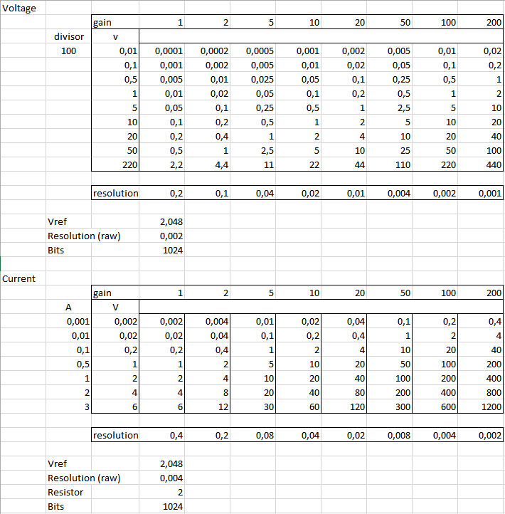
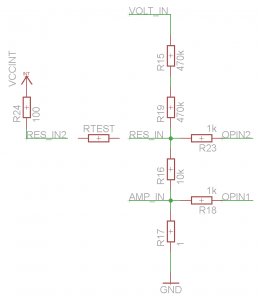
So here’s the input circuitry I came up with:
it should be able to measure both current and voltage at the same time, to calculate instant power consumption.
Time to test the PGA!
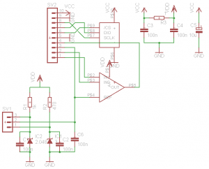
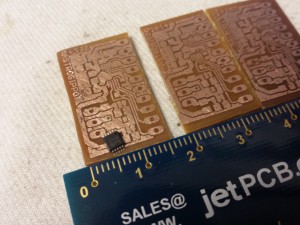
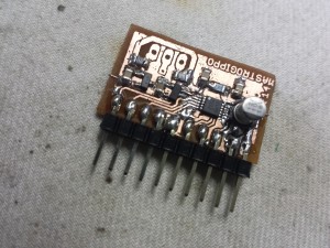
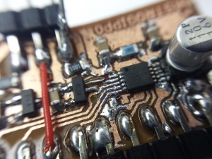
The PGA113 comes in a VSSOP package so I just decided to build a simple breakout board with the basic passives required to make the device work. I also included two precision voltage reference sources, selectable with a jumper.
The board has only one single jumper wire, so it can be printed on a single layer of a dual-layer PCB, keeping the back as a ground plane.
Everything worked on the first try! The PGA113 is quite simple to work with, and the datasheet is clear and complete; it was just a simple matter of modifying the SPI/digitalPot example to send the right two bytes, and I had my PGA working!
// include the SPI library:
#include <SPI.h>

#define PGA_CS 10

void setup()
{
pinMode (PGA_CS, OUTPUT);
SPI.begin();

SetPGA(0,0);
}

void loop()
{
}

void SetPGA(int G, int Ch) {
  //take the SS pin low to select the chip:
  digitalWrite(PGA_CS, LOW);
  //send in the address and value via SPI:
  SPI.transfer(0x2A);
  SPI.transfer((G<<4) + Ch);
  //take the SS pin high to de-select the chip:
  digitalWrite(PGA_CS, HIGH);
}
That’s it! Now on to the 3310 PCB design!
